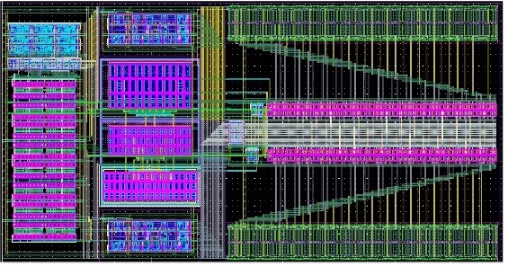
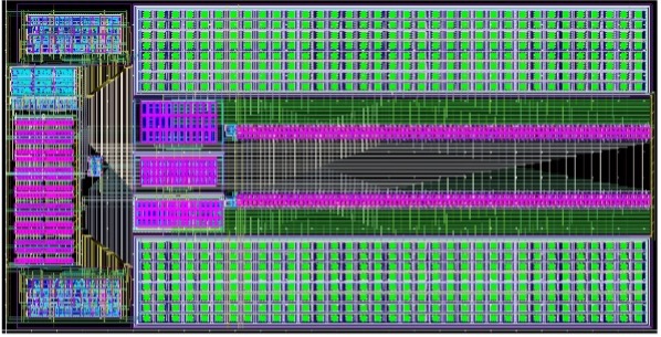
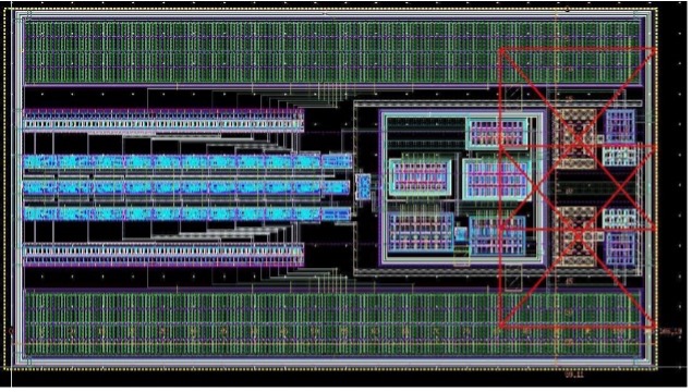
Silicon-Proven Designs
Our collection of successfully taped out IPs and chips, demonstrating expertise across analog, digital, and mixed-signal domains.
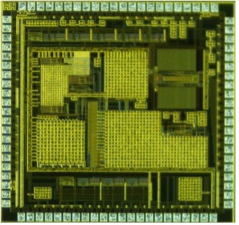
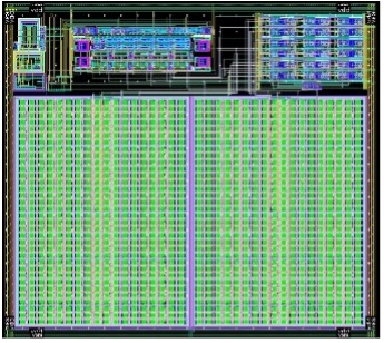
50 kS/s, Synchronous Cyclic Integration-Based Impedance Measurement IC for EIT
A high-accuracy impedance measurement IC achieving 99.7% accuracy and 50 kS/s throughput, designed for broadband bio-impedance sensing. It employs a synchronous cyclic integration technique with a scalable capacitive transimpedance stage, enabling single-cycle I/Q demodulation without requiring an analog LPF. Fabricated in 180-nm CMOS, the IC operates from 100 Hz to 100 kHz while consuming just 50 μW from a 1.2 V supply.
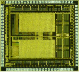
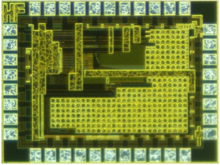
100 kS/s, Baseline-Canceling, Peak-Based Impedance Measurement IC for EIT
A high-throughput impedance measurement IC with less than0.1% baseline resolution and 100 kS/s frame rate, designed for neural Electrical Impedance Tomography (EIT) applications. The IC features a baseline-canceling peak detector that resets each cycle to a known DC level, enabling accurate extraction of small impedance changes riding on large signal baselines. Fabricated in a 180-nm CMOS process, the design supports a frequency range of 100 Hz to 100 kHz while consuming only 31–39 μW from a 1.2 V supply. The compact IC achieves a die area of 3.182 mm².
1–75 mA, 20 mV Dropout, Analog-Assisted Fast Transient Digital LDO
A digital low dropout (DLDO) regulator, with less than 0.14mV steady-state voltage ripples (VRIPP) and a minimum dropout voltage of 20 mV, for driving both noise-sensitive analog and power-efficient digital load circuits in system-on-chip circuits. The Silicon proven DLDO is designed in 180-nm CMOS process with a die area of 0.253 mm2. The DLDO achieves a line regulation of 8 mV/V and a load regulation of 0.081 mV/mA while driving a maximum ILOAD of 75 mA with a peak current efficiency of 99.93%.
10-bit, Differential SAR-Based Voltage-Mode DELTA Cap DAC Asynchronous ADC with S/H
A 10-bit differential SAR-based voltage-mode Asynchronous ADC with sample-and-hold (S/H) and power-down features, designed for low-power operation in a 65nm process. Supports differential inputs with a VINP/VINN swing of ~1 V around a common-mode voltage, delivers an ENOB of 9.1, and has a gain error of 20%. Operating with quiescent current (IDD) of 1 μA, the design includes a serializable digital output port (DOUT) with I/O levels from 0 to VDD. The compact layout occupies 96 x 84 µm2.
10-bit, Differential SAR-Based Voltage-Mode TSMC Cap DAC Asynchronous ADC with S/H
A 10-bit differential SAR-based voltage-mode Asynchronous ADC with sample-and-hold (S/H) and power-down features, designed for low-power operation in a 65nm process. Supports differential inputs with a VINP/VINN swing of ~1 V around a common-mode voltage, delivers an ENOB of 9.7, and has a gain error of 30%. Operating with 15 KHz input bandwidth and quiescent current (IDD) of 1.5 μA, the design includes a serializable digital output port (DOUT) with I/O levels from 0 to VDD. The compact layout occupies 112 x 101 µm2.
0.5–160 mA, 20 mV Dropout, Fast Transient Digital LDO
A digital low dropout (DLDO) regulator, with ≤0.13mV steady-state voltage ripples (VRIPP) and a minimum dropout voltage of 20 mV, for driving both noise-sensitive analog and power-efficient digital load circuits in system-on-chip circuits. The Silicon proven DLDO is designed in 180-nm CMOS process with a die area of 0.22 mm2. The DLDO achieves a line regulation of 4 mV/V and a load regulation of 0.01 mV/mA while driving a maximum ILOAD of 160 mA with a peak current efficiency of 99.96%.
Differential SAR-Based Voltage-Mode Asynchronous ADC with S/H
This IP is a low-power, 10-bit asynchronous differential voltage ADC with integrated sample-and-hold and power-down features. It supports ~1 V peak-to-peak input swing around a 0.5×VDD common-mode voltage and includes an optional serialized digital output. The asynchronous architecture enables dynamic reduction of digital power in steady-state conditions. Designed in 65 nm technology, it achieves ~9.2 ENOB with ~1.2 µA current consumption and a 15 kHz input bandwidth.
Differential SAR-Based Voltage-Mode Synchronous ADC with S/H
This IP is a low-power, 8-bit synchronous differential voltage ADC with integrated sample-and-hold and power-down features. It supports ~1 V peak-to-peak input swing around a 0.5×VDD common-mode voltage and includes an optional serialized digital output. The synchronous architecture enables dynamic reduction of digital power in steady-state conditions. Designed in 65 nm technology, it achieves ~7.1 ENOB with ~0.8 µA current consumption and a 25 kHz input bandwidth.
Differential SAR-Based Voltage-Mode Synchronous ADC with S/H
This IP is a low-power, 8-bit synchronous differential voltage ADC with integrated sample-and-hold and power-down features. It supports ~1 V peak-to-peak input swing around a 0.5×VDD common-mode voltage and includes an optional serialized digital output. The synchronous architecture enables dynamic reduction of digital power in steady-state conditions. Designed in 65 nm technology, it achieves ~7.3 ENOB with ~0.9 µA current consumption and a 25 kHz input bandwidth.
Differential SAR-Based Voltage-Mode Synchronous ADC with S/H
This IP is a low-power, 8-bit synchronous differential voltage ADC with integrated sample-and-hold and power-down features. It supports ~1 V peak-to-peak input swing around a 0.5×VDD common-mode voltage and includes an optional serialized digital output. The synchronous architecture enables dynamic reduction of digital power in steady-state conditions. Designed in 65 nm technology, it achieves ~7.5 ENOB with ~1.1 µA current consumption and a 25 kHz input bandwidth.
100 MS/s 10-bit SAR ADC with 9.68 ENOB in a Compact, Low-Power Design
This 10-bit Successive Approximation Register (SAR) ADC is optimized for low power consumption and high-speed operation, achieving an effective number of bits (ENOB) of 9.68 at a sampling rate of 100 MS/s. Designed using a 65-nm CMOS technology, the ADC occupies a compact active area of just 0.0062 mm². It utilizes a minimal sampling capacitance of 1.04 pF, contributing to its energy efficiency. The total power consumption is remarkably low at 0.746 mW while maintaining high-speed performance at 100 MS/s.